⬅️ Part 1: Embracing the Challenge - System Architecture Overview
Building upon Part 1, this section provides a deeper dive into the process of mapping the massive 1.55 billion gate Atom chip emulation onto a multi-FPGA prototyping platform. We’ll examine the key engineering challenges we faced and the innovative solutions we developed, specifically focusing on strategies for conquering routing congestion, implementing manual partitioning, and integrating essential debug and scalability features.
1. System Overview and Hardware Foundation
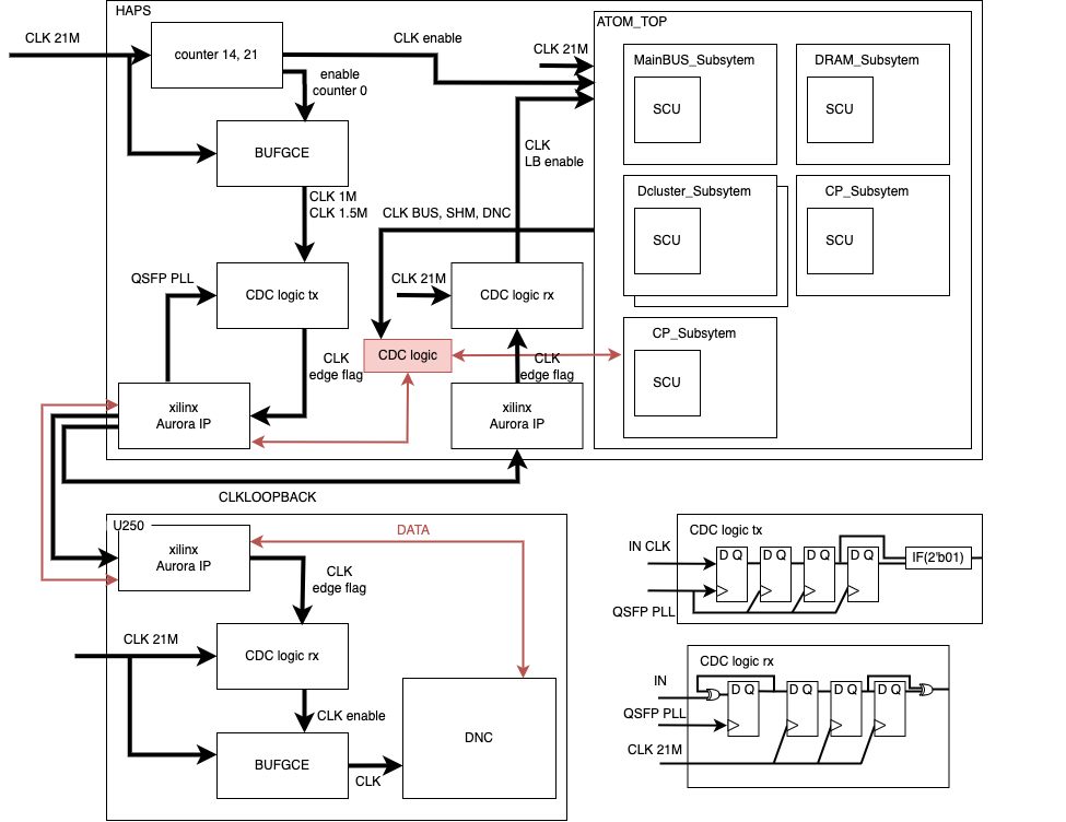
- Prototyping Platform: A hybrid system comprising a HAPS-100 (housing 2 VU19P FPGAs: uB, uC) and 9 supplementary Xilinx U250 boards (1 for Shared Memory/DRAM, 8 for the Distributed Neural Engine).
- Emulation Objective: To achieve cycle-accurate emulation of the Atom chip, enabling thorough pre-silicon validation.
- Core Design Principle: Functional partitioning of the Atom chip across multiple FPGAs, strategically maximizing inter-FPGA communication bandwidth while carefully managing on-chip resources.
2. Ensuring Synchronous Multi-FPGA Operation: Clock and Reset Distribution
A cornerstone of accurate emulation is maintaining synchronous operation across all FPGAs. This requires a precisely engineered clock and reset distribution system. Unlike ASIC methodologies that rely on automated flows (SDC, PIPD), multi-FPGA designs demand explicit and optimized inter-FPGA signal propagation. Our solution employed Xilinx Aurora IP as the high-speed physical layer, upon which we built a custom protocol for distributing synchronized clock and reset signals across the entire system.
3. Functional Partitioning Strategy
The allocation of specific Atom chip functions to individual FPGAs was a critical design decision, directly impacting performance and routability.
HAPS-100 – Centralized Control and Interconnect
- VU19P uB (Network-on-Chip - NOC): This FPGA was dedicated to implementing the Atom chip’s complex Network-on-Chip (NoC). Given the NoC’s size and central role in inter-block communication, isolating it onto a dedicated FPGA was crucial for managing routing complexity.
- VU19P uC (Neural Engine Cluster & Control Processor - NECluster, CP): This FPGA housed the primary computational element, the Neural Engine Cluster (NECluster), alongside the Control Processor (CP) Subsystem responsible for overall system orchestration. Grouping these control and compute functions together optimized communication pathways.
Xilinx U250s – Scalable Memory and Compute Resources
- U250 (Shared Memory & DRAM - SHM/DRAM): A single U250 board provided a scalable off-chip Shared Memory and DRAM subsystem, effectively extending the limited on-chip SRAM available within the FPGAs.
- U250 (Distributed Neural Engine - DNC): To handle the immense computational demands of the Atom chip, eight U250 boards were configured as a Distributed Neural Engine (DNC). This parallel processing architecture allowed for scalable compute power necessary for emulation.
4. Tackling Implementation Bottlenecks: Routing Congestion and Resource Optimization
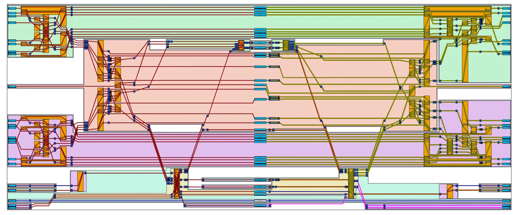
a. Manual Partitioning and HSTDM-Driven Routing Optimization
While the HAPS-100 toolchain offers automated partitioning, achieving the required performance and routability for a design of this scale necessitated a manual, optimization-driven approach.
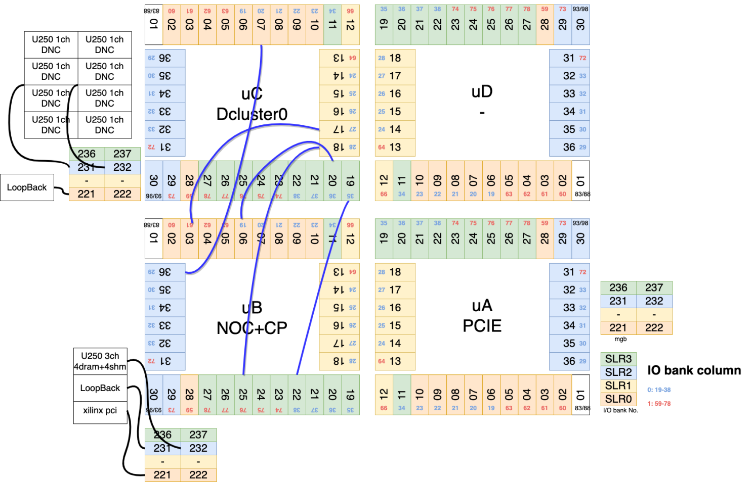
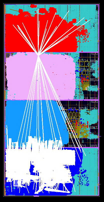
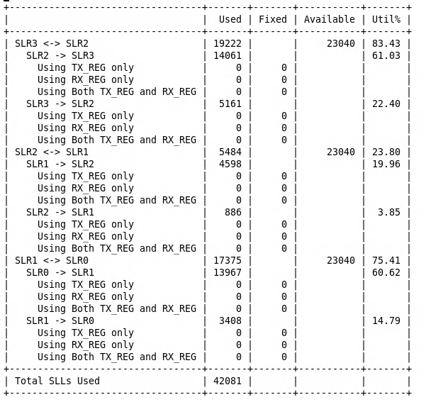
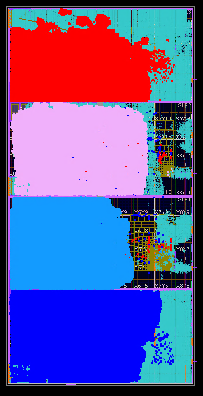
- The Challenge: Managing Inter-FPGA Data Flow via HSTDM: A primary hurdle was efficiently managing the high-bandwidth data streams crossing between FPGAs using Synopsys’ HSTDM (High-Speed Time-Division Multiplexing) technology. Crucially, the physical placement of these HSTDM transceivers within the VU19P FPGAs – specifically, their assignment to optimal SLRs – had a profound impact on routing success.
- SLR Placement: A Critical Factor: Each VU19P SLR (Super Logic Region) possesses dedicated LVDS and HSIO resources. However, inter-SLR communication within a VU19P incurs significant routing penalties and resource overhead. Minimizing these SLR boundary crossings became a paramount objective.
- Protocompiler Limitation: Lack of Direct LVDS Constraint: Synopsys Protocompiler, while powerful, does not provide direct mechanisms to precisely control the assignment of HSTDM channels to specific LVDS pins. This limitation required us to develop an indirect, iterative optimization strategy.
- Iterative HSTDM Optimization and Constraint Generation:
- Constraint Complexity: Generating effective constraints was challenging due to the intricacies of differential signaling and TDM module associations. Constraints had to enforce signal directionality (e.g., “uA” FPGA transmit to “uB” FPGA receive) and correctly link signals to appropriate HSTDM modules (e.g., “HSTDM_128”).
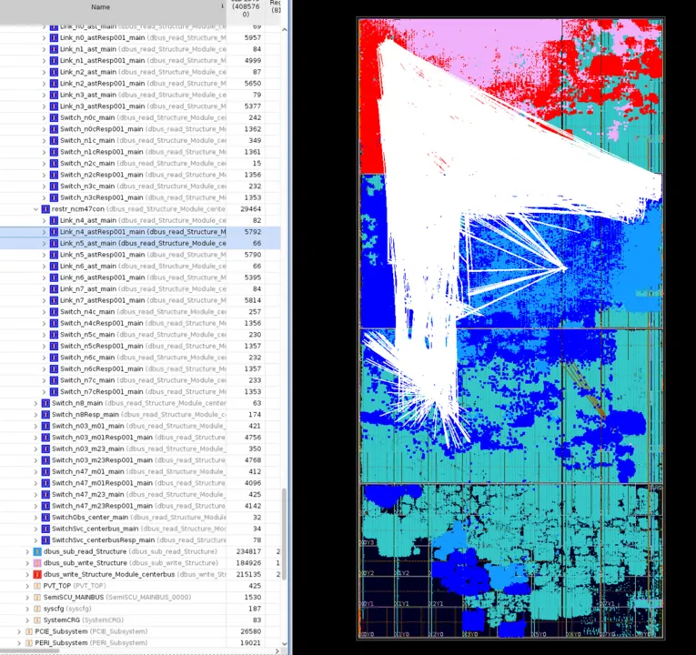
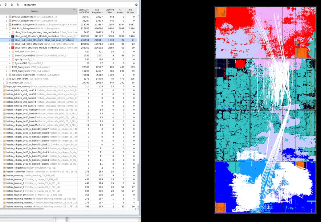
- Outcome: Streamlined Interconnect and Reduced Congestion: This iterative HSTDM optimization and constraint-driven approach dramatically improved routing efficiency. The initial “spaghetti” routing, characterized by interwoven read/write AXI signals chaotically crossing SLRs, was transformed into a cleaner, more structured design with minimized SLR crossings and significantly reduced congestion.
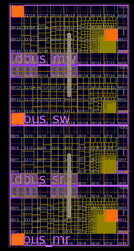
b. SLR Partitioning and SSI Bandwidth Management
- Persistent Routing Congestion: The 128-bit AXI Bottleneck: Even with optimized HSTDM placement, the 128-bit width of the main NOC AXI bus presented a persistent routing challenge. The sheer volume of signals, particularly within the VU19P’s limited SLL (Slice Logic LUT) interconnect and across the relatively constrained SSI (Stacked Silicon Interconnect) links between SLRs, threatened implementation feasibility. The Main Bus alone accounted for approximately 13,000 nets (
10 * (1024(data)+200(address/control))). - NOC Hierarchical Architecture and SSI Limitations: The Atom chip’s NoC employed a two-layer hierarchy.
- Initial Mapping Bottleneck: Our initial mapping strategy, placing each NoC layer within a single SLR, proved unsustainable. The massive inter-layer net count overwhelmed the limited SSI bandwidth between VU19P SLRs, creating a severe routing bottleneck. The SSI links became a critical choke point.
Simple SERDES code for reducing SSI:
module simple_serial_16x#(
  parameter PWIDTH = 1024,
  parameter SWIDTH = 64
)(
    input clk,
    input [PWIDTH-1:0] din_parallel,
    output [SWIDTH-1:0] dout_serial,
    output data_en
);
localparam NUM_WORD = PWIDTH / SWIDTH;
    reg [$clog2(NUM_WORD)-1:0] addr;
    reg [PWIDTH-1:0] dout;
    reg data_en_reg;
    always @(posedge clk)
        addr<=addr+1;
    always @(posedge clk) begin
        dout <= din_parallel[addr*SWIDTH+:SWIDTH];
        data_en_reg=&addr;
    end
    assign data_en=data_en_reg;
    assign dout_serial = dout;
endmodule

module simple_deserial_16x#(
  parameter PWIDTH = 1024,
  parameter SWIDTH = 64
)(
    input clk,
    input [SWIDTH-1:0] din_serial,
    output [PWIDTH-1:0] dout_parallel,
    input data_en
);
localparam NUM_WORD = PWIDTH / SWIDTH;
    reg [$clog2(NUM_WORD)-1:0] addr;
    reg [PWIDTH-1:0] dout;
    always @(posedge clk)
        addr<=(data_en)?0:addr+1;
    always @(posedge clk)
        dout[addr*SWIDTH+:SWIDTH] <= din_serial;
    assign dout_parallel=dout;
endmodule
c. Enhancements for Debug and Scalability
Beyond routing optimization, we proactively incorporated features to enhance debug capabilities and future system scalability:
Embedded Xilinx ILA (Integrated Logic Analyzer): Extensive use of Xilinx ILAs throughout the design provided critical real-time visibility into signal behavior, enabling efficient debugging of complex interactions and timing-critical paths.
Integrated MicroBlaze Soft Processor: A MicroBlaze processor was embedded for on-chip system management, monitoring, and potential runtime configuration, adding a layer of system observability and control.
Comprehensive JTAG Access (Internal & External): Both internal and external JTAG interfaces were implemented, providing versatile access for system-level debug, boundary scan testing, and potential future hardware expansion or modification.
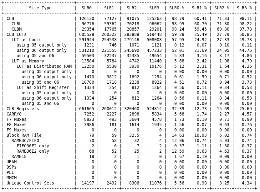
5. Emulation System Performance and Resource Utilization
6. Terminology Glossary
HAPS-100: Synopsys’s FPGA-based hardware prototyping system, typically incorporating multiple Xilinx FPGAs (in our case, VU19Ps).
VU19P: Xilinx Virtex UltraScale+ VU19P – Xilinx’s largest FPGA, notable for its multi-die (SLR) architecture and SSI interconnect.
SLR (Super Logic Region): A die-level partition within an SSI-based FPGA like the VU19P, offering distinct routing and resource characteristics.
SSI (Stacked Silicon Interconnect): The technology enabling high-bandwidth die-to-die communication within Xilinx SSI-based FPGAs.
HSTDM (High-Speed Time-Division Multiplexing): Synopsys’s proprietary TDM solution for efficient inter-FPGA data transfer, utilizing dedicated HT3 LVDS bundles.
AXI (Advanced eXtensible Interface): A widely used high-performance interface standard for on-chip communication.
LVDS (Low-Voltage Differential Signaling): A standard for high-speed, low-power differential signaling commonly used in FPGA interconnects.
HSIO (High-Speed Serial I/O): General term for high-speed serial transceivers in FPGAs, often used for chip-to-chip communication.
SDC (Synopsys Design Constraints): A standard format for specifying timing and physical constraints in ASIC and FPGA design flows.
JTAG (Joint Test Action Group): An industry-standard interface for testing and debugging hardware systems.