


1. NPU 메모리 아키텍처: 왜 Cache보다 Scratchpad인가?
NPU(Neural Processing Unit) 설계에서 가장 먼저 마주하는 아키텍처적 선택지는 “데이터를 어떻게 관리할 것인가"입니다. 저는 이 지점에서 일반적인 CPU의 방식이 아닌, NPU 특화된 메모리 구조를 선택했습니다.
CPU vs NPU: 결정론적 데이터 흐름의 차이
- 일반적인 CPU: 실행 경로가 복잡하고 분기 예측(Branch Prediction)이 어려워 데이터 접근 패턴이 매우 불규칙합니다. 따라서 하드웨어가 실시간으로 데이터를 관리하고 교체하는 L1/L2 Cache 구조가 필수적입니다.
- NPU: 행렬 곱셈(Matrix Multiplication)과 같은 딥러닝 연산은 반복적이며 데이터의 흐름이 매우 결정론적(Deterministic)입니다. 즉, 어떤 데이터가 어느 시점에 필요할지 컴파일러 단계에서 미리 완벽하게 알 수 있습니다.
Scratchpad Memory(SPM)의 전략적 이점
이러한 결정론적 특성 덕분에 NPU에서는 하드웨어가 알아서 관리하는 캐시보다, 소프트웨어가 직접 제어하는 Scratchpad Memory(SPM) 방식이 훨씬 유리합니다.
- 면적 최적화: 캐시에 필수적인 하드웨어 Tag 로직과 데이터 비교 로직을 제거할 수 있습니다. 여기서 아낀 면적은 더 많은 연산기나 더 큰 메모리 용량을 확보하는 데 사용됩니다.
- 최고의 효율성: Google의 TPU나 Tenstorrent와 같은 선도적인 NPU 기업들이 SPM 방식을 선호하는 핵심 이유입니다. 소프트웨어가 메모리 배치를 직접 관리함으로써 불필요한 데이터 교체를 방지하고 전력 효율을 극대화합니다.
우리 설계의 계층 구조: Scratchpad + Shared Memory
저희 설계에서는 데이터 재사용성을 높이기 위해 저장 공간을 두 가지 레이어로 세분화했습니다.
- Scratchpad (Local): 각 연산 코어가 독립적으로 사용하여 고속 연산을 지원하는 로컬 저장소.
- Shared Memory (Shared): 여러 연산 코어가 반복적으로 필요한 데이터를 공유하고 재사용하여 외부 메모리(DRAM) 접근을 최소화하는 공유 공간.
이러한 이중 구조는 NPU 내부의 데이터 흐름을 최적화하고, 전체 시스템 성능을 끌어올리는 든든한 기반이 됩니다.
2. NPU 내부 저장소 설계의 핵심: 면적과 성능의 줄타기
NPU는 수많은 연산 코어가 동시에 대량의 데이터에 접근하여 연산을 수행하는 구조입니다. 이 때문에 NPU 내부 저장소는 전체 칩 면적의 상당 부분을 차지하며, ‘제한된 면적 내 최대 용량 확보’는 곧 칩의 경쟁력과 직결됩니다.
하지만 단순히 용량만 늘리는 것은 불가능합니다. 여러 코어가 반복적으로 데이터 요청을 보내는 환경에서 최적의 성능을 보장하기 위해서는 메모리 액세스 속도 또한 매우 중요하기 때문입니다. 저는 이번 프로젝트에서 NPU의 핵심 저장 공간인 Shared Memory를 설계하며 면적과 성능을 동시에 만족시키기 위한 최적화 작업을 진행했습니다.
특히 신경 썼던 부분은 Read Cache 구현과 Test Interface (Shared Bus) 설계였습니다. SRAM의 동작 주파수와 주변 로직의 속도 차이를 극복하기 위해 Read Cache를 도입했고, 무엇보다 테스트를 위한 로직이 실제 동작(Functional) 경로의 타이밍에 미치는 악영향을 최소화하기 위해 노력했습니다.
3. 기술적 과제: 이전 설계의 한계와 STA 타이밍 손해 분석
SRAM을 Die 내에 고밀도로 배치하면서도 안정적인 테스트를 보장하는 것은 매우 까다로운 작업입니다. 이전 과제에서는 일반적인 ASIC 설계 방식에 따라 MBIST(Memory Built-In Self Test) 로직을 SRAM 바로 앞에 배치하는 방식을 사용했습니다. 하지만 이 방식은 물리적 설계(Physical Design) 단계에서 심각한 문제점을 드러냈습니다.
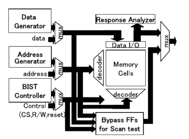 그림 0은 Memory BIST의 기본적인 동작 원리를 보여줍니다. SRAM 메모리 외부에 BIST Controller가 존재하며, Test Mode일 때 Mux를 통해 Test Pattern (Address, Data, Control)을 SRAM으로 공급하고, 출력된 데이터를 기대값과 비교하여 불량 여부를 판단합니다. 이 Mux가 실제 동작 경로상에 위치한다는 점이 핵심입니다.
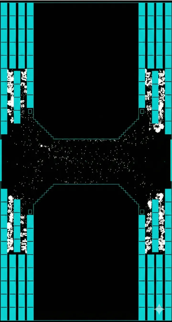
그림 1 이전 ATOM 과제의 실제 레이아웃을 확인해보면, 수많은 SRAM Macro 사이사이에 BIST 로직(Controller 및 Collars)들이 산재해 있는 것을 볼 수 있습니다. 이처럼 BIST 로직이 SRAM 근처에 위치하게 되면, 실제 동작(Functional) 신호가 이동해야 할 경로에 Mux가 추가되면서 STA(Static Timing Analysis) 결과가 급격히 나빠집니다.
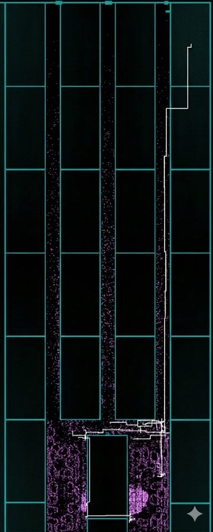
그림 2는 이러한 타이밍 손해의 물리적인 이유를 명확히 보여줍니다. SRAM Macro 사이의 공간(Channel)은 매우 좁아 테스트 로직이 들어갈 충분한 공간이 나오지 않습니다. 이로 인해 테스트 로직과 Mux는 SRAM에서 다소 먼 곳에 배치될 수밖에 없고, 여기서 SRAM까지 신호를 전달하기 위해 수많은 Buffer와 Inverter Chain이 필수적으로 추가됩니다. 이 ‘불필요한 꼬리’들이 엄청난 타이밍 지연을 유발합니다.
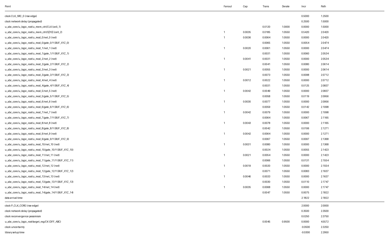
그림 3 실제 STA Report를 분석해본 결과, 테스트 Mux 이후에도 무려 14단의 Buffer를 통과해야 하는 것을 확인할 수 있었습니다. 이는 Functional Read Path에 엄청난 Timing Penalty를 가져왔고, 전체 시스템의 동작 주파수를 올리는 데 큰 걸림돌이 되었습니다.
4. 해결책: Shared Bus 기반 설계 변경 및 면적 최적화
저는 이러한 문제를 근본적으로 해결하기 위해 Mentor(Siemens)의 Shared Bus 인터페이스를 도입했습니다. 핵심 아이디어는 테스트 로직을 SRAM 바로 앞이 아니라, 타이밍 여유가 있는 Regslice(Pipeline Stage) 앞쪽으로 전진 배치하는 것입니다. 이는 제 이전 경력인 삼성 CPU Hardening 프로젝트에서의 경험을 ASIC 설계에 접목한 결과입니다.
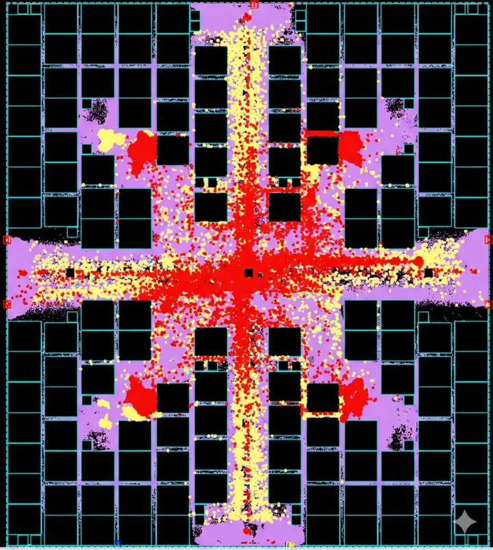
Shared Bus 방식을 적용한 새로운 Shared Memory 영역의 DFT(Scan, BIST) 로직 분포를 확인해보면, SRAM Macro 사이 영역에 로직이 거의 존재하지 않는 것을 볼 수 있습니다. SRAM 근처에서 타이밍 Critical한 Mux와 Buffer들을 제거했기 때문에 가능했습니다. 그 결과, SRAM Macro를 훨씬 더 조밀하게 배치할 수 있었고, 동일 면적 내에 더 많은 SRAM을 집적할 수 있었습니다.
5. 결과 및 비교 분석: 숫자로 증명하는 최적화 효과
설계 변경 결과는 합성(Synthesis) 및 레이아웃 단계에서 극적으로 나타났습니다.
| 항목 | 기존 방식 (Screatch Pad 적용) | 개선 방식 (Shared Bus 적용 SHM) |
|---|---|---|
| Mux Count | 27,000개 | 14,000개 (약 48% 절감) |
| Timing | Buffer Chain으로 인한 Critical | Regslice 전진 배치로 Margin 확보 |
| Area Density | 로직 분산으로 SRAM 간격 벌어짐 | SRAM 밀집 배치 가능 (Max Capacity) |
| IR Drop/Power | 좁은 공간 로직 밀집으로 IR Drop 악화 | 균일한 분포로 파워 문제 개선 |
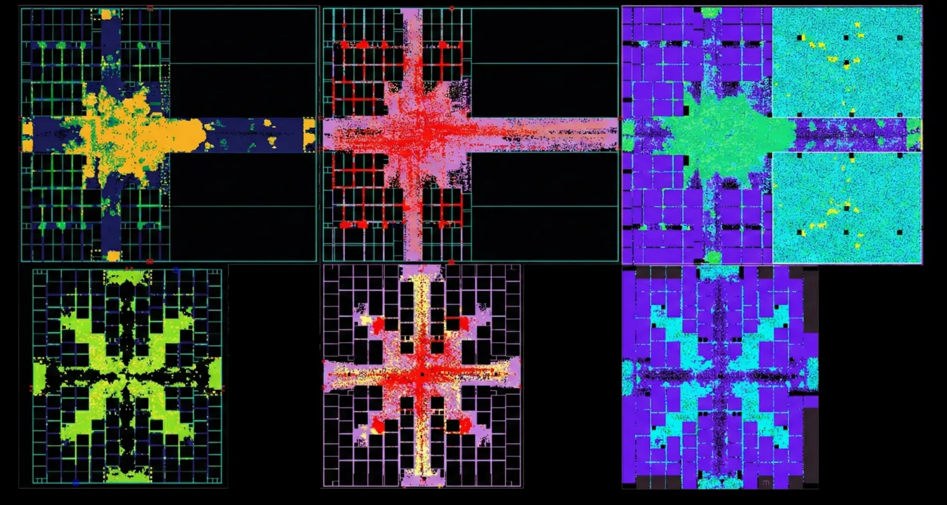 그림 5: Scratch Pad vs Shared Memory 물리적 특성 비교 (붉은색일수록 분포가 높음) > * a, d: Cell Density Map
- b, e: DFT Logic Location (노란색: Scan, 붉은색: BIST)
- c, f: DVD (Dynamic Voltage Drop) Map
그림에서 보듯이, Shared Bus가 적용되지 않은 Screatch Pad 영역은 SRAM Macro 사이에 BIST 로직들이 다수 존재하여, Cell Density가 비정상적으로 높고, 좁은 공간에 배치된 로직들로 인해 파워 문제(DVD Drop)까지 발생합니다.
반면, 제가 설계한 Shared Bus 적용 Shared Memory 영역은 SRAM 사이 공간이 매우 깨끗하여, Cell Density가 고르게 분포하며, DVD 파워 문제 또한 현저히 개선된 것을 확인할 수 있습니다.
6. 마치며: 하드닝 경험이 ASIC 설계에 주는 가치
이번 최적화 과제는 단순히 DFT 기능을 구현하는 것을 넘어, 물리적 레이아웃과 타이밍 슬랙을 고려한 아키텍처 설계가 얼마나 중요한지를 보여주는 좋은 사례였습니다. ARM CPU 설계 등에서 사용되는 High-end Hardening 기법을 제가 직접 ASIC 설계에 적용함으로써 Mux 27K -> 14K 감소라는 놀라운 면적 최적화를 달성할 수 있었습니다.
앞으로도 저희 팀은 제한된 칩 면적 내에서 NPU의 성능을 극대화하기 위해, 물리적 설계를 고려한 다양한 아키텍처적 시도를 계속해 나갈 것입니다. 감사합니다.
1. NPU Memory Architecture: Why Scratchpad over Cache?
The very first architectural decision encountered in NPU (Neural Processing Unit) design is “how to manage data.” At this juncture, I opted for an NPU-specific memory architecture rather than the conventional CPU approach.
CPU vs. NPU: The Difference in Deterministic Data Flow
- Conventional CPUs: With complex execution paths and difficult branch prediction, data access patterns are highly irregular. Therefore, an L1/L2 Cache structure, where hardware manages and replaces data in real-time, is essential.
- NPUs: Deep learning operations, such as matrix multiplication, are repetitive, and the data flow is highly deterministic. In other words, the compiler knows exactly what data will be needed and when.
The Strategic Advantage of Scratchpad Memory (SPM)
Thanks to this deterministic nature, software-controlled Scratchpad Memory (SPM) is vastly superior in NPUs compared to hardware-managed caches.
- Area Optimization: The hardware Tag logic and data comparison logic, which are essential for caches, can be eliminated. The area saved here is utilized to secure more compute units or larger memory capacity.
- Maximum Efficiency: This is the core reason why leading NPU companies like Google (TPU) and Tenstorrent prefer the SPM approach. By having software directly manage memory allocation, unnecessary data replacement is prevented, and power efficiency is maximized.
Our Design’s Hierarchical Structure: Scratchpad + Shared Memory
To increase data reusability, we subdivided the storage space into two distinct layers in our design.
- Scratchpad (Local): Local storage used independently by each compute core to support high-speed operations.
- Shared Memory (Shared): A shared space where multiple compute cores share and reuse repeatedly needed data, thereby minimizing external memory (DRAM) access.
This dual structure optimizes the data flow inside the NPU and serves as a robust foundation for boosting overall system performance.
2. The Core of NPU Internal Storage Design: Balancing Area and Performance
An NPU is structured so that numerous compute cores simultaneously access massive amounts of data to perform operations. Because of this, internal storage takes up a significant portion of the total chip area, and “maximizing capacity within a limited area” directly translates to the chip’s competitiveness.
However, simply increasing capacity is not viable. In an environment where multiple cores repeatedly send data requests, guaranteeing optimal performance requires extremely fast memory access speeds. During this project, I undertook optimization efforts to simultaneously satisfy both area and performance requirements while designing the Shared Memory, the NPU’s core storage space.
Particular attention was given to implementing the Read Cache and designing the Test Interface (Shared Bus). To overcome the speed discrepancy between the SRAM’s operating frequency and the surrounding logic, a Read Cache was introduced. Above all, I focused on minimizing the adverse impact of the test logic on the timing of the actual functional paths.
3. Technical Challenges: Limitations of Previous Designs and STA Timing Penalty Analysis
Ensuring stable testing while densely placing SRAMs within the die is a highly demanding task. In a previous project, we followed standard ASIC design practices by placing MBIST (Memory Built-In Self Test) logic directly in front of the SRAM. However, this approach revealed severe issues during the Physical Design stage.
Figure 0 illustrates the basic operating principle of Memory BIST. A BIST Controller exists outside the SRAM memory. In Test Mode, it supplies Test Patterns (Address, Data, Control) to the SRAM via a Mux and judges pass/fail by comparing the output data with expected values. The critical point is that this Mux is located directly on the actual functional path.
Looking at the actual layout of the previous ATOM project in Figure 1, you can see BIST logic (Controllers and Collars) scattered among numerous SRAM Macros. When BIST logic is located near the SRAM like this, Muxes are added to the paths where actual functional signals must travel, causing Static Timing Analysis (STA) results to deteriorate sharply.
Figure 2 clearly shows the physical reason for this timing penalty. The spaces (Channels) between SRAM Macros are too narrow to accommodate the test logic. Consequently, the test logic and Muxes are forced to be placed somewhat far from the SRAM. To transmit signals from there to the SRAM, numerous buffers and inverter chains must inevitably be added. These ‘unnecessary tails’ cause massive timing delays.
As analyzed in the actual STA Report in Figure 3, signals had to pass through a staggering 14 stages of buffers even after the test Mux. This introduced a tremendous timing penalty to the Functional Read Path and became a major bottleneck in increasing the overall system operating frequency.
4. The Solution: Shared Bus-Based Design Modification and Area Optimization
To fundamentally resolve this issue, I introduced Mentor’s (Siemens) Shared Bus interface. The core idea is to move the test logic forward—not right in front of the SRAM, but ahead of the Regslice (Pipeline Stage) where there is more timing margin. This is the result of applying my previous experience from Samsung CPU Hardening projects to ASIC design.
Checking the new DFT (Scan, BIST) logic distribution in the Shared Memory area where the Shared Bus was applied, you can see almost no logic exists in the areas between the SRAM Macros. This was possible because timing-critical Muxes and buffers near the SRAM were removed. As a result, we could pack the SRAM Macros much more densely, integrating more SRAM within the same area.
5. Results and Comparative Analysis: Optimization Effects Proven by Numbers
The results of the design changes manifested dramatically during the synthesis and layout stages.
| Metric | Previous Method (Applied to Scratchpad) | Improved Method (SHM with Shared Bus) |
|---|---|---|
| Mux Count | 27,000 | 14,000 (Approx. 48% Reduction) |
| Timing | Critical due to Buffer Chains | Margin secured by advancing Regslice |
| Area Density | Logic dispersion widened SRAM gaps | Dense SRAM placement possible (Max Capacity) |
| IR Drop/Power | Worsened IR Drop due to logic crowding in narrow spaces | Power issues improved through uniform distribution |
Figure 5: Physical characteristic comparison between Scratchpad and Shared Memory (The redder, the higher the density)
- a, d: Cell Density Map
- b, e: DFT Logic Location (Yellow: Scan, Red: BIST)
- c, f: DVD (Dynamic Voltage Drop) Map
As shown in the figure, the Scratchpad area (without the Shared Bus) has numerous BIST logics between SRAM Macros, resulting in abnormally high Cell Density. The logics crammed into narrow spaces even trigger power issues (DVD Drop).
In contrast, the Shared Memory area where I applied the Shared Bus design is very clean between the SRAMs. You can clearly see that the Cell Density is evenly distributed, and the DVD power issues have also been significantly mitigated.
6. Conclusion: The Value of Hardening Experience in ASIC Design
This optimization project was a prime example showing how critical architectural design is when considering physical layout and timing slack, going far beyond merely implementing DFT functions. By directly applying high-end hardening techniques used in ARM CPU design to this ASIC design, I achieved an astonishing area optimization, reducing the Mux count from 27K to 14K.
Moving forward, our team will continue to experiment with various architectural approaches that consider physical design to maximize NPU performance within a limited chip area. Thank you.